The Biggest Difference Between GPUs vs TPUs
An overview of Nvidia's switched fabric vs Google's 3d torus

The big breakthrough for Nvidia’s newest generation of Blackwell GPUs was the introduction of the GB200 NVL72 rack.
Previously, Nvidia servers included just 8 GPUs in each node. With GB200 NVL72, that number shot up to (you guessed it) 72.
You can think of a “node” as the largest group of GPUs that are all directly linked together. Frontier models today are too big to fit on a single GPU, and when you’re using multiple GPUs to run an LLM, performance is often bottlenecked by the speed of your GPU-to-GPU communications.
For Nvidia, GPUs within a node are connected using NVLink, their fastest interconnect technology. Once you start going across nodes, you get downgraded to Infiniband/Ethernet, which is well over 10x slower.
Traditional Moore’s law is dead, and we can no longer count on chip-level innovations alone to continue the beautiful exponential. Entire datacenters are the new unit of compute. GB200 NVL72 9x-ed the number of GPUs within a single node, and networking is increasingly cited as one of Nvidia’s largest moats. It’s no wonder why “AI factory” and “extreme co-design” have become Jensen Huang’s new favorite phrases.1
But, if you look at the spec sheet for Google’s latest TPU v7, you’ll notice something interesting… “number of chips per pod = 9216.”
9216!? Can Google link 128x more chips in a node than Nvidia!?! Is Nvidia totally cooked!?!?!
Of course not! The truth is that Google and Nvidia use two totally different networking topologies. It’s probably the biggest difference between TPUs vs GPUs.
Why care about networking at all?
Before we dive into the specifics of Google vs Nvidia, it might be useful to provide some background on why networking matters in the first place.
Networking is broadly defined as how to link all your chips together. It’s what transforms a bunch of isolated XPUs into a “coherent cluster” that can simultaneously work on the same problem.
To transfer data between two XPUs, you need to connect them with a physical cable. Networking speeds today are already often the bottleneck for AI workloads, and wireless communication is 100x slower.
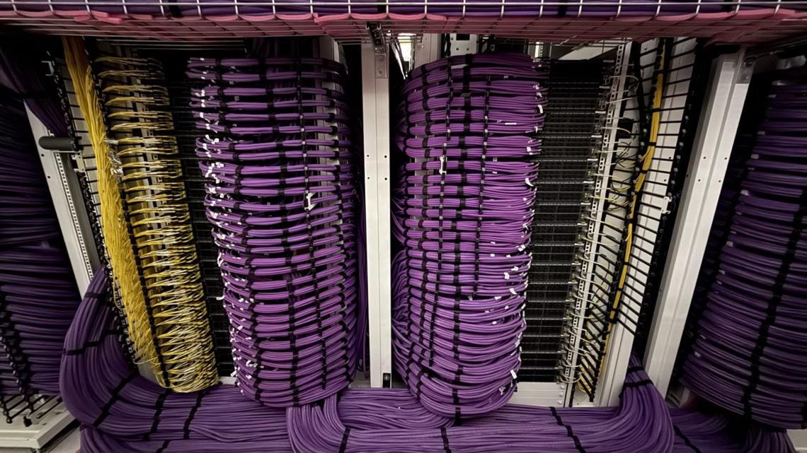
The most straightforward thing to do would be to directly connect each XPU to every other XPU. This is called a “full mesh” network, and it works when your cluster is small.
The largest AI datacenters today, however, have hundreds of thousands of XPUs and are rapidly growing. If you wanted to use a full mesh network with 200,000 XPUs, each one would need 199,999 ports connected using ~20 billion cables.
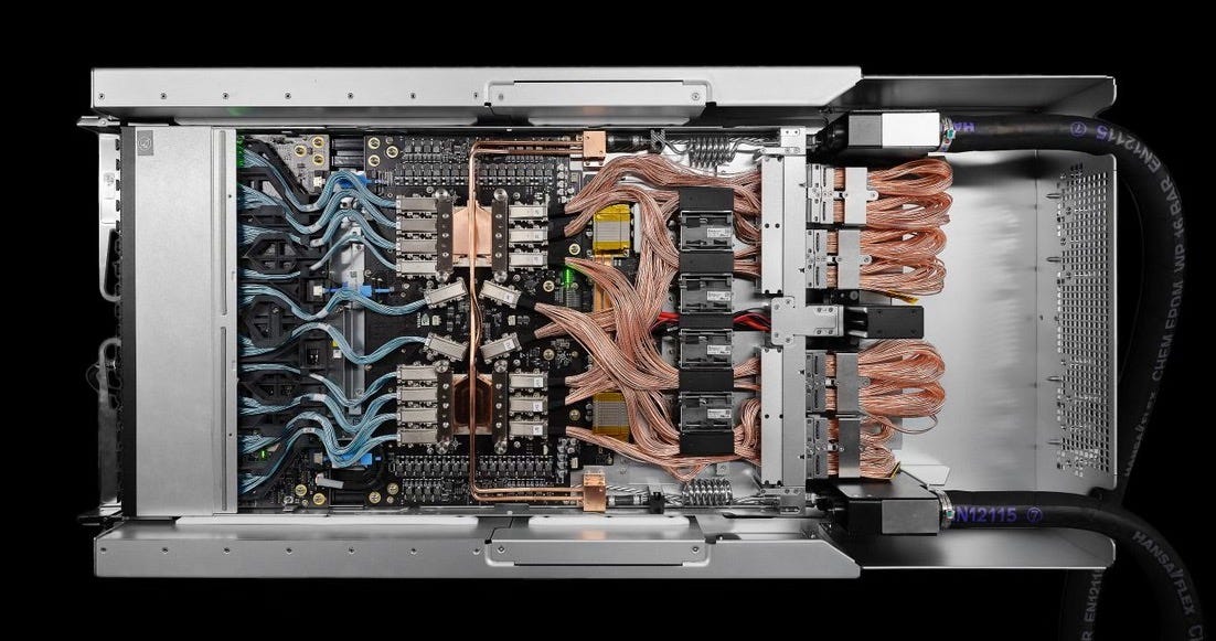
Obviously that isn’t going to work, and this is where network topology comes in. It’s how you connect hundreds of thousands of GPUs together while keeping the whole system efficient and performant.
Google and Nvidia have chosen two totally different methods to scale their XPU clusters. Let’s take a closer look below.
Nvidia’s switched fabric
The first step of Nvidia’s networking strategy is to “scale up” as many GPUs in a single node as possible. Previously, we mentioned how a node consists of the largest group of GPUs that are all directly connected to one another. You can think of it like trying to create one giant GPU.
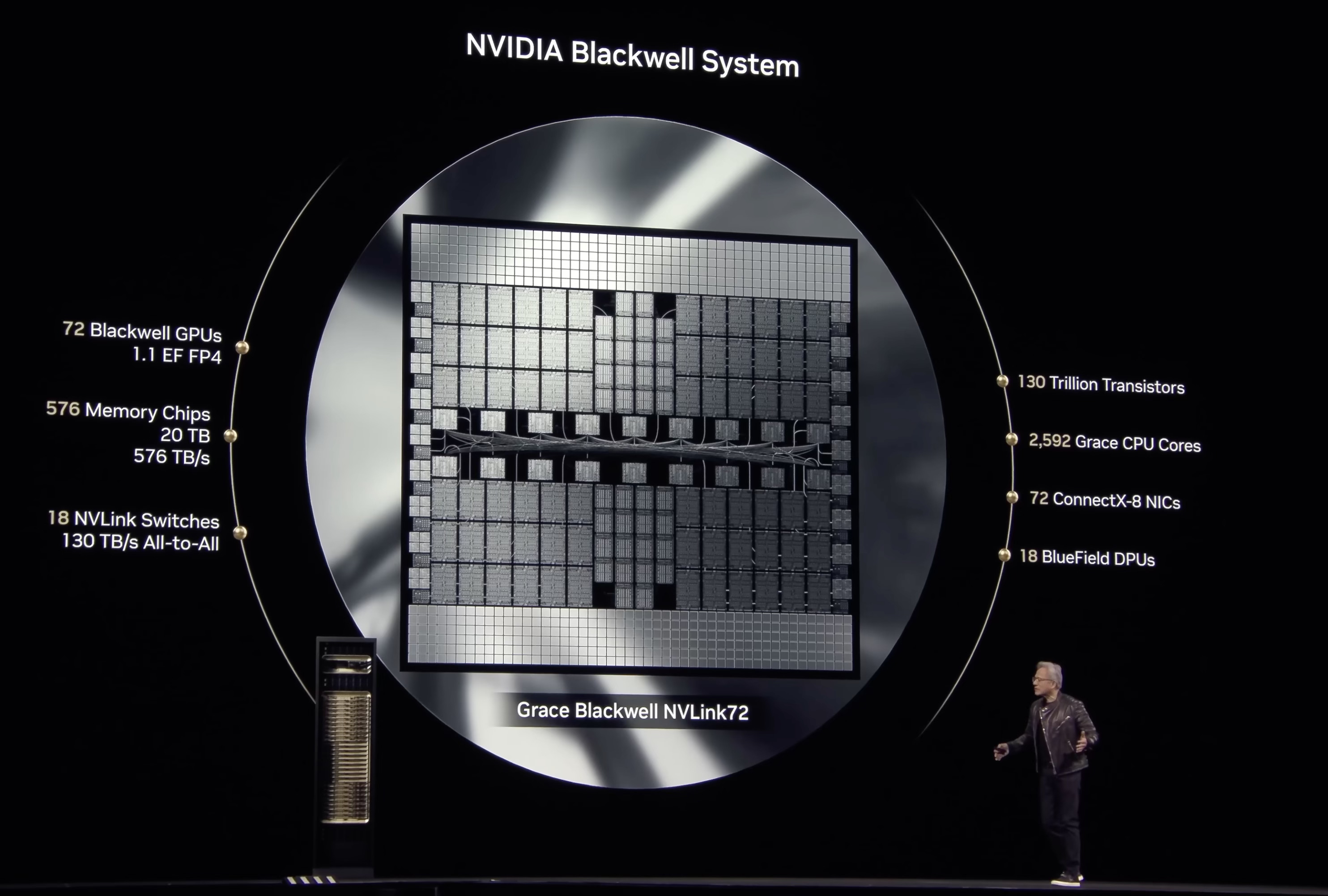
A “switch” is a hardware device designed specifically to route data between other devices. They’re what give the “switched fabric” its name.
Within a node, Nvidia uses their fastest proprietary switches to connect each GPU to every other GPU. It’s called NVLink and is used exclusively for scale up.2
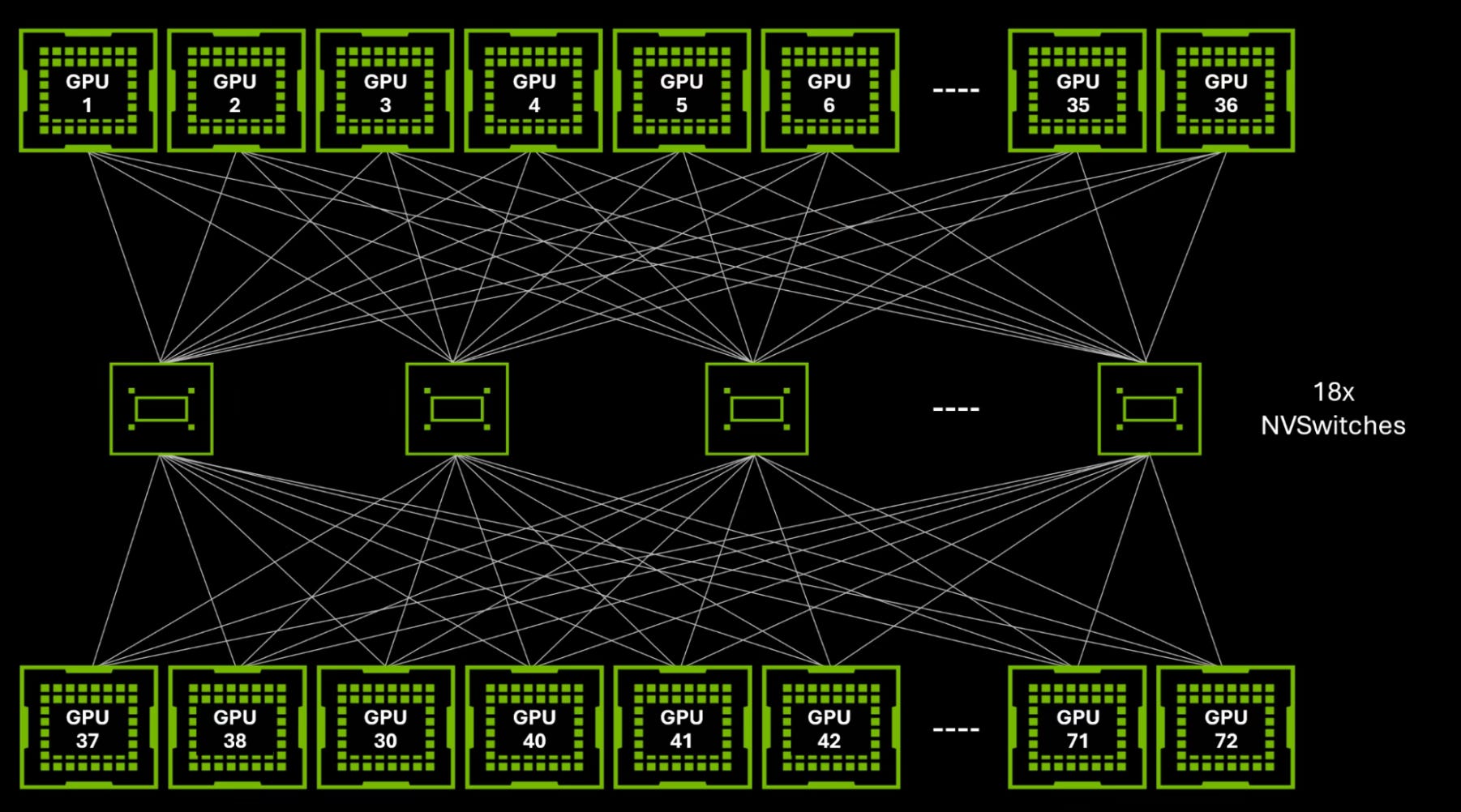
The next step is to “scale out” by connecting all your nodes together.
Here, switches are used as well, but they follow the industry standard InfiniBand/Ethernet protocols. Both are dozens of times slower than NVLink in exchange for being able to traverse much longer distances.
Nvidia makes their own InfiniBand and Ethernet switches, and they’re of course suggested as the default options for scaling out their GPUs. However, you can use 3rd party switches from companies like Cisco, Arista, Juniper, etc as well.3 You can also use Nvidia switches with non-Nvidia GPUs.
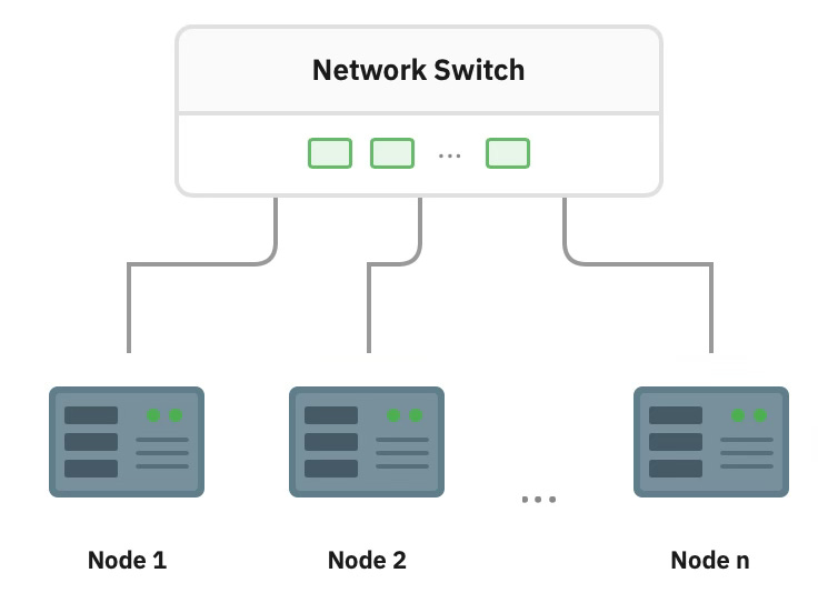
Top of the line network switches (generic term for Ethernet or InfiniBand) typically have 64 ports, so a single switch can only get you so far. The natural solution is to add more switches that route data between other switches, and that’s exactly what we do.
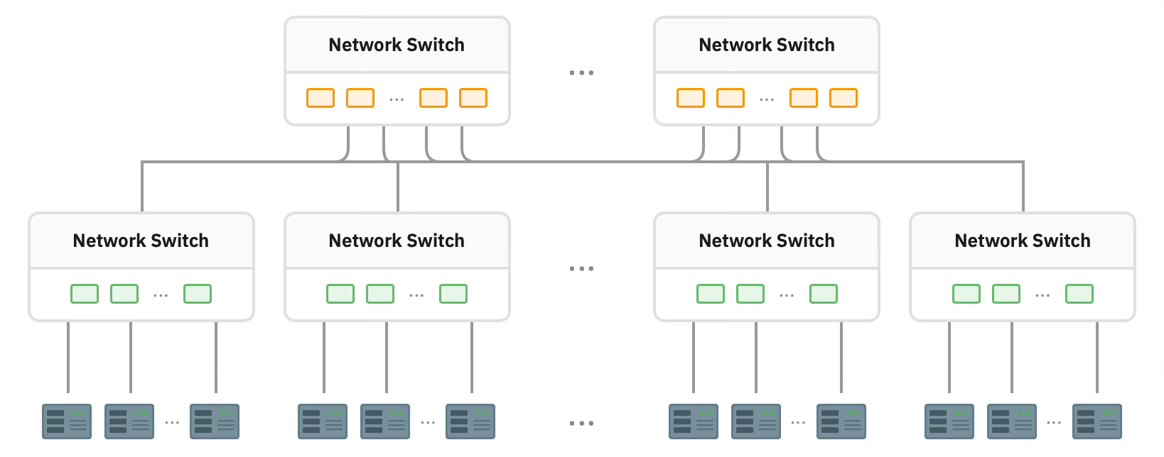
This two layer switch structure is called a “spine-leaf architecture,” and it’s the backbone of most modern datacenters. The top level switches are spines and the ones below them are leaves.
To communicate between any two nodes, you only need two hops from leaf → spine → leaf.
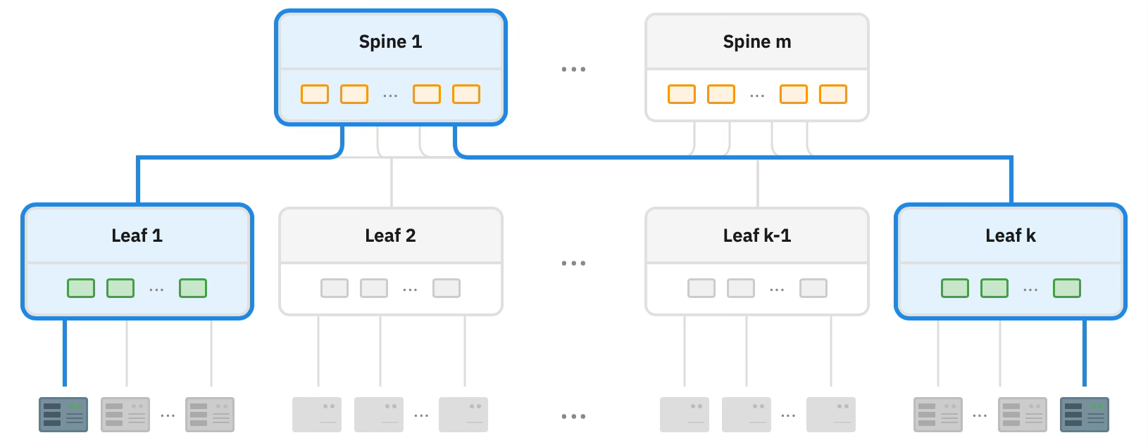
You might be wondering why we have multiple spines connected to every leaf. Isn’t one spine enough to guarantee that each pair of nodes is only two hops away from each other?
That’s absolutely correct, but remember that interconnect speeds are determined by physical cables connecting your switches and GPUs. If we add a second spine connected to every leaf, we’re effectively doubling the total bandwidth between our spines and leaves (assuming you double the number of cables as well of course). It’s also useful for system resiliency.
Here’s Nvidia’s reference architecture for a full GB200 SuperPOD Scalable Unit. It offers 576 connected GPUs for the low low price of 30-40 million dollars.
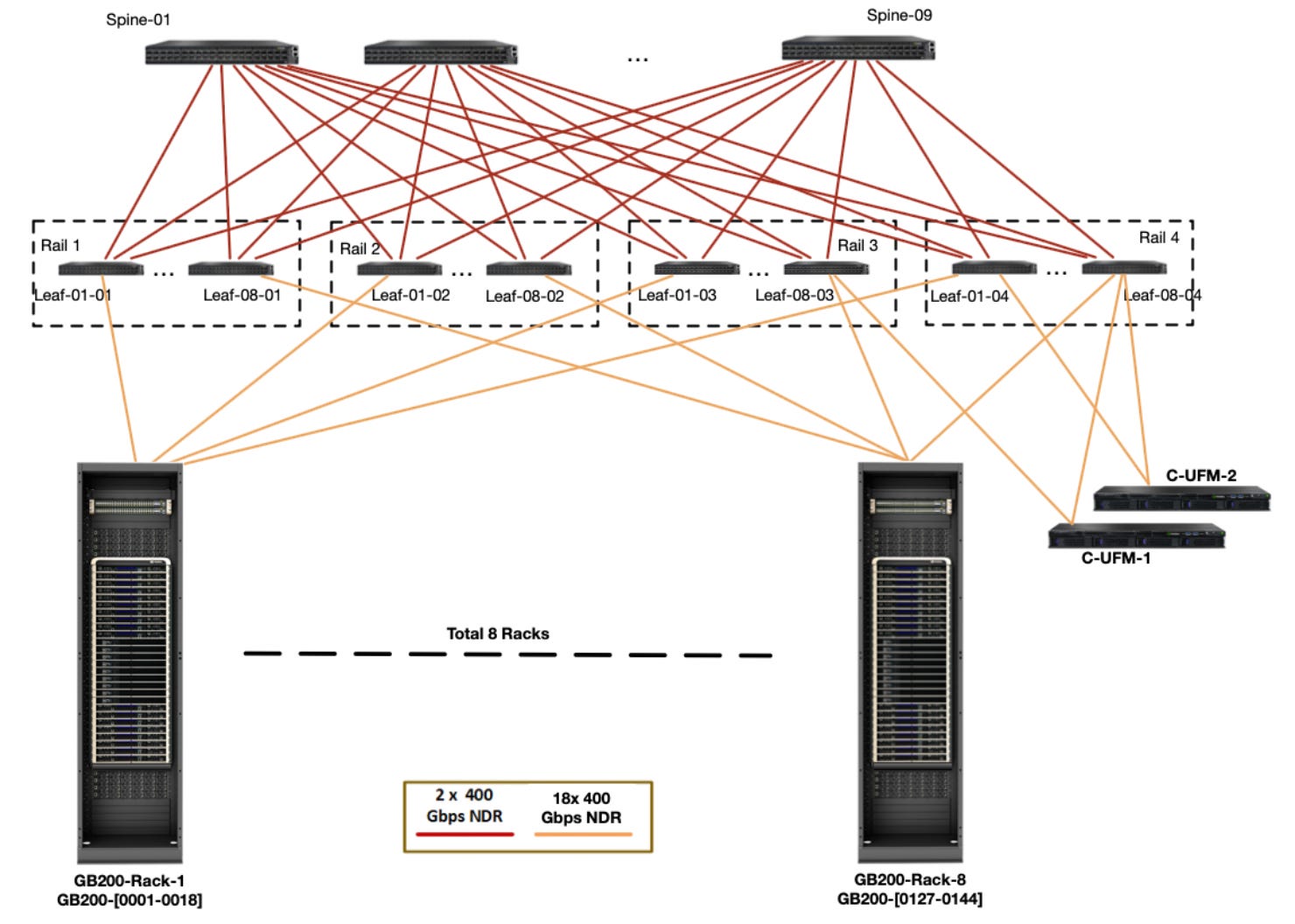
The picture is a little more complicated than our toy diagrams, but you should be able to recognize the main components! We have 8 GB200 NVL72 nodes at the bottom which are connected to 32 leaf switches. Those leaf switches are then connected to 9 spine switches.
For those who’re curious, I’ll explain the other parts of the diagram in the footnotes.4
If you wanted to expand beyond 576 GPUs, you’d add another layer of switches above the spines. Nvidia calls these “core switches,” and using their reference architecture would bring you to 9,216 GPUs for a measly ~600 million dollars.
Beyond that point, there’s no longer a reference architecture. I’m assuming you’d either add yet another layer of networking switches or use a different fabric with a looser set of rules to link your 9,216 GPU megapods.
Google and their 3d torus
We’ve repeatedly mentioned that 9x-ing the number of GPUs that are all directly connected to one another was Nvidia’s big innovation for Blackwell.
Google, on the other hand, doesn’t even try connecting every pair of TPUs at all.
Instead, each of their racks consists of a 4x4x4 cube of 64 TPUs.
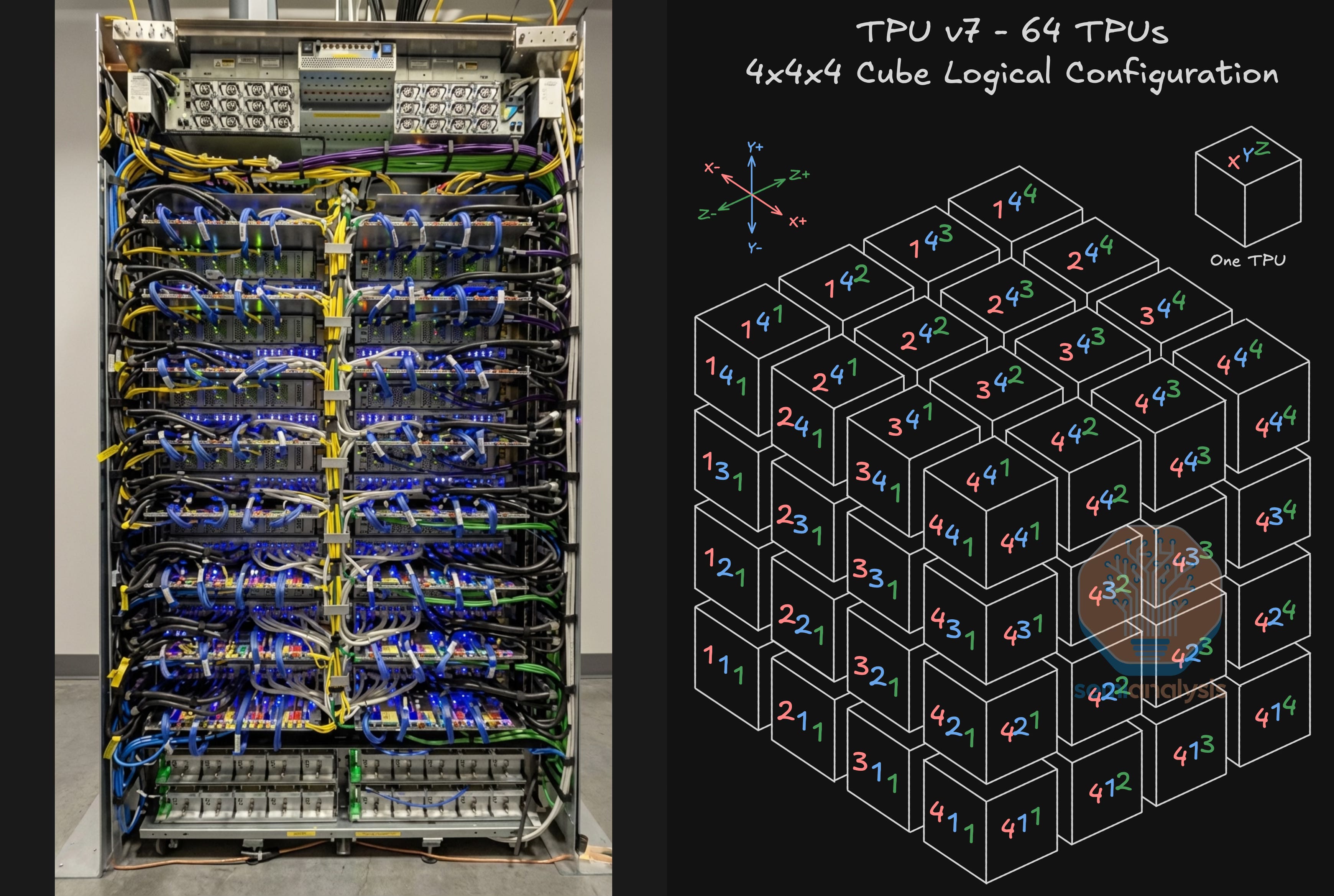
Each TPU is connected to each of its 6 direct neighbors—2 on each of the X, Y, and Z axes. This includes TPUs on the outer faces, edges, and corners! In these cases, the connection wraps around to the corresponding face/edge/corner on the opposite side of the cube.
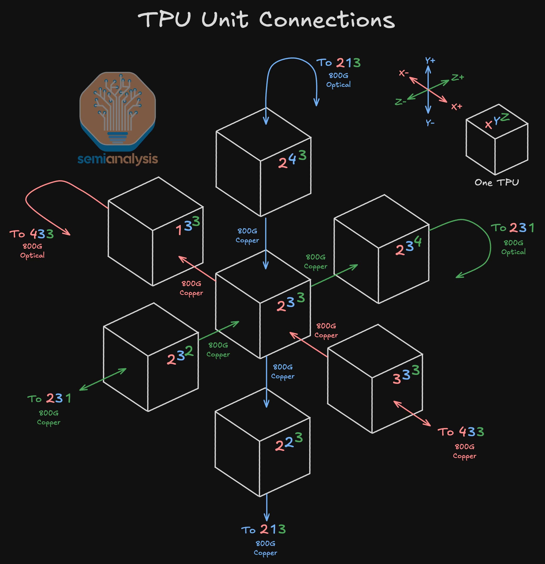
These wraparound links are what make the interconnect topology a “3d torus”.5 Importantly, they reduce the maximum distance between any two TPUs from N to N/2. Faces have 1, edges have 2, and corners have 3. Interior TPUs, of course, have 0.
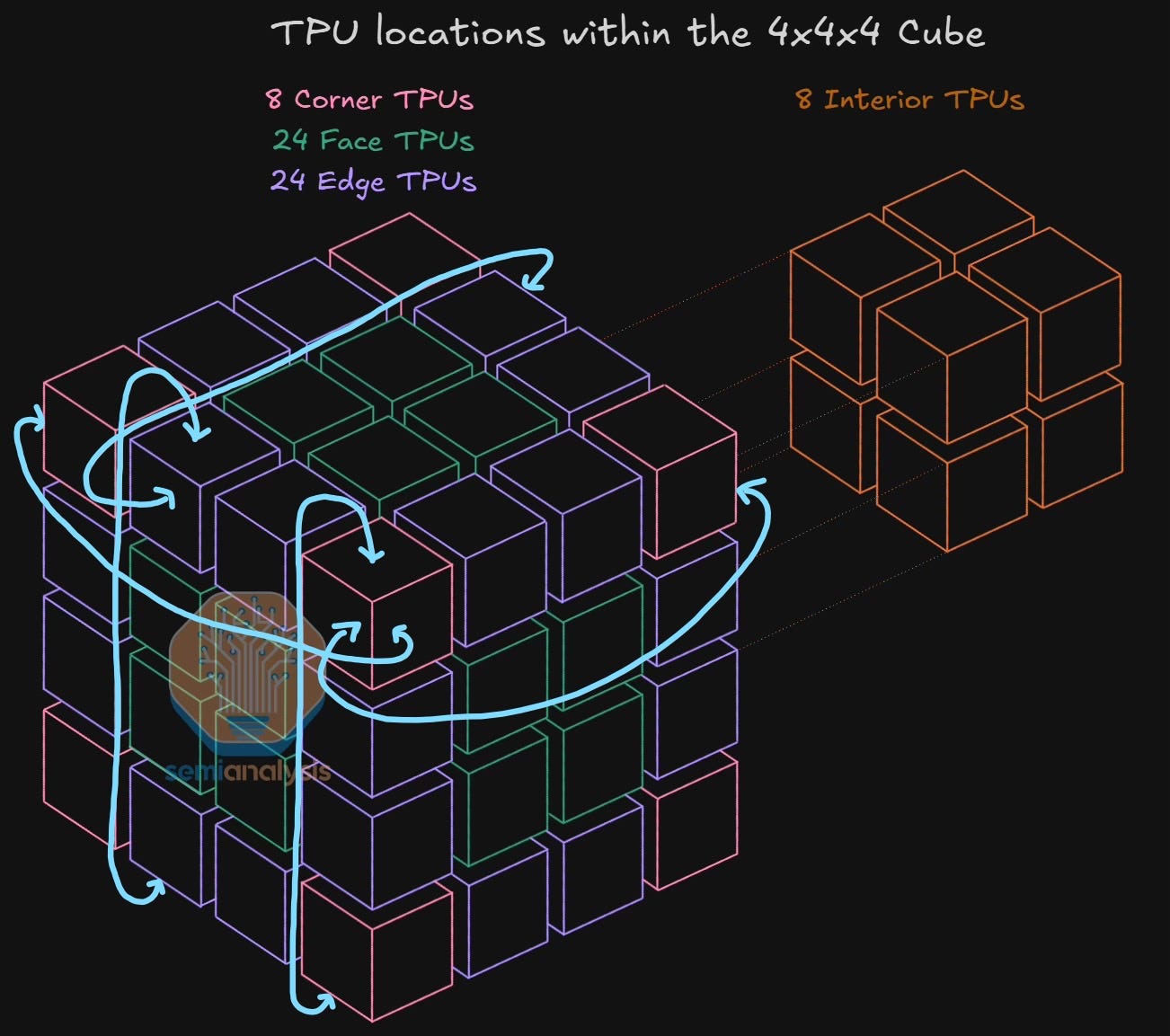
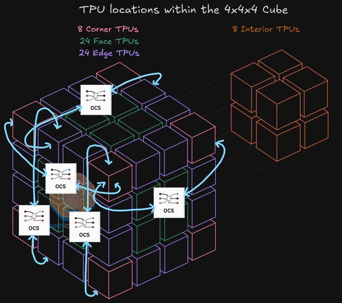
For non-wraparound links, the TPUs are truly directly connected to each other using copper cables.6 Logically, it’s best to think of the wraparound links as direct connections as well, but the two TPUs are actually connected to an intermediate Optical Circuit Switch (OCS) using fiber optic cables.
Unfortunately, the word “switch” is overloaded here. OCSes are very different from the network switches we discussed earlier. Network switches can route data to/from all of the cables connected to them simultaneously. In contrast, OCSes can only connect each inbound cable to exactly one outbound cable.
More specifically, you can think of each OCS as having exactly N inbound connections and N outbound connections. The setup is actually very flexible because you can use software to dynamically connect any inbound connection to any outbound connection in milliseconds. However, each inbound connection can crucially only be connected to exactly 1 outbound connection at any given point in time.
This 4x4x4 cube is only phase one of scaling up TPUs. Phase two is linking many cubes together.
Google hasn’t publicly said how many OCSes the 9,216 TPUv7 superpod uses, but if we extrapolate from their TPU v4 paper, it should be exactly 48.
Why 48?
Each cube has 6 faces with 4x4 = 16 OCS endpoints each for a total of 96. I like to think of each of these endpoints as being uniquely defined by an index (1-16), axis (X, Y, Z), and direction (+, -). As you can see from the above diagram, the two endpoints with the same index and axis but opposite directions are connected to the same OCS.
In other words, if we were to give each pair of endpoints—e.g. (1, X, -) and (1, X +)—their own OCS, we would end up with 96/2 = 48 OCSes.
For a single cube, this feels a bit wasteful. After all, the main point of OCSes are that they can programmatically connect any of their N input connections to any of their N output connections, and with just 1 cube, N = 1.
The magic happens when we add more cubes. As long as our OCS has enough ports, we can connect each pair of same index same axis endpoints from all of our cubes to the same OCS.7 This allows us to dynamically connect the (1, X, -) endpoint from cube A to the (1, X, +) endpoint of any other cube in our network! Generalize the same principle across all the other endpoints, and you can essentially combine each cube with any other cube on demand. The only requirement is that the two faces need to be along the same axis and opposite directions (e.g. you can attach any +Y face to any -Y face).
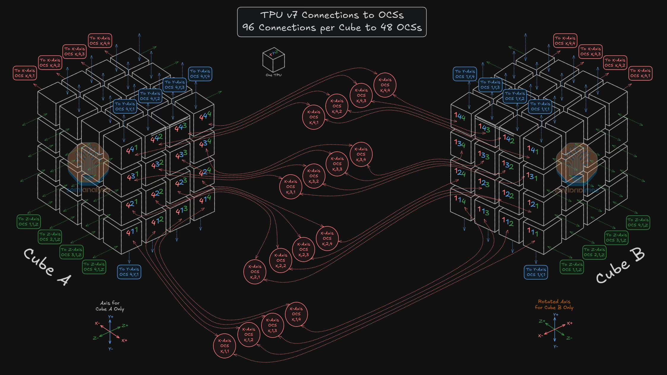
This entire scale up system that links up to 9,216 TPUs with their 6 direct neighbors is called Inter-Chip Interconnect (ICI). You’ll also hear the word “slice” used to refer to a group of TPUs connected using ICI. Google’s unfortunately inconsistent with their terminology here, but I think both “pod” and “superpod” generally refer to the maximum possible slice size.
The final step is to scale out by linking multiple pods together.
To do this, Google uses a separate data center network (DCN) called Jupiter. Jupiter is to scale out what ICI is to scale up.
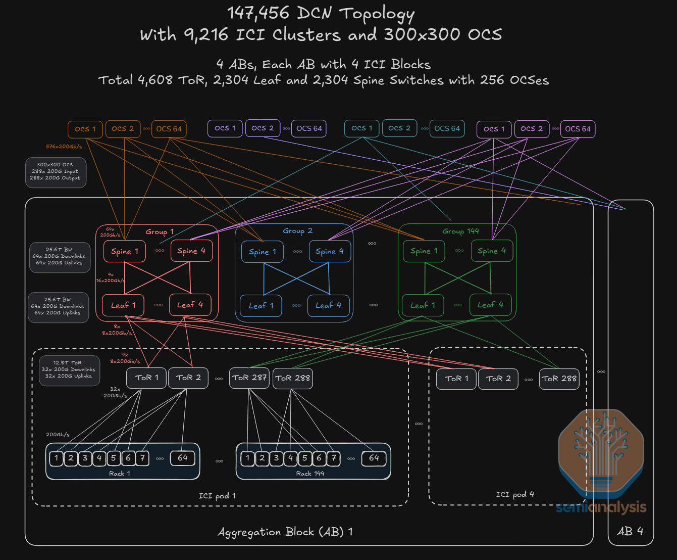
The exact Jupiter setup used for TPU v7 is not publicly known, but the general idea is to first connect multiple pods into a single “aggregation block” (AB) using a traditional spine-leaf architecture with Ethernet switches, and then connect multiple ABs together using OCSes.
These top-level OCSes play a similar role to the OCSes inside each pod. They essentially allow you to dynamically redistribute bandwidth between different ABs.
How these networking differences actually affect the bottom line
To summarize, Nvidia’s networking philosophy is to (1) create the largest node possible where every GPU is directly linked to every other GPU and then (2) use a large number of network switches to minimize the number of hops between any two nodes.
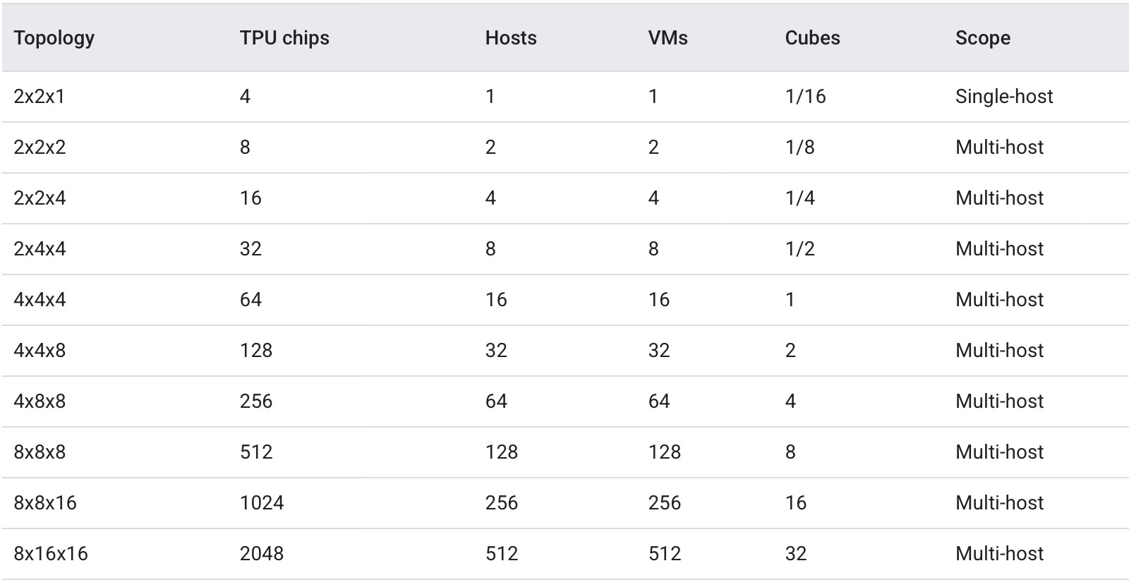
Google, on the other hand, is ok with each TPU only being linked to its 6 direct neighbors. The most obvious benefit of this more modular system—as we just saw with the 9,216 TPU superpod—is that it’s easier to scale to much larger world sizes.
OCSes also allow you to easily reconfigure the network however you want. There are thousands of different slice sizes to choose from, and if there’s something wrong with a TPU or two, you can simply route around them.
The price for this increased flexibility is ease of use. A 3d torus is generally harder to reason about than a traditional switched fabric because the exact location of your data can significantly affect performance.
As one example, AlltoAll is a very common collective used when working with frontier LLMs that takes a set of GPUs and has each GPU send a different chunk of data to every other GPU. Having a node where every pair of GPUs is directly connected is literally perfect for this! In contrast, to do the same thing with a 3d torus, you need to think very carefully about where exactly all the relevant data sits in the torus, how many hops apart they are, avoiding congestion during transfers, etc.
This brings us to the most important metric: total cost of ownership (TCO) per unit of performance.
The marketed performance for a B200 vs TPUv7 is extremely similar.
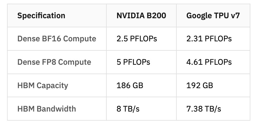
However, according to Semianalysis, the TCO for TPUv7—for a 3rd party customer like Anthropic—is ~30% cheaper than GB200s. Part of this is because of Nvidia’s eye watering 75% gross margins, but it’s also partly because NVLink switches are very expensive.
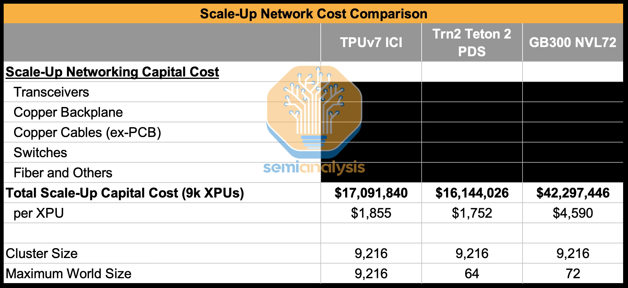
In other words, if you can achieve a similar percentage of peak theoretical performance (the marketed specs for chips are always bs) on both accelerators, then TPUs will truly be cheaper than GPUs.
Unfortunately, percentage of peak theoretical performance varies a lot depending on workload (input/output sequence length, desired latency, etc) and how smart your engineers are.
For the vast majority of potential customers, it’s almost certain that TCO per unit of performance will be worse for TPUs than GPUs. The entire open source ML ecosystem is optimized for Nvidia GPUs, and the average engineer does not know how to use a 3d torus. If you try running Deepseek R1 today using vanilla PyTorch + vLLM on GB200s vs TPU v7s, Nvidia will win. This is the famed CUDA moat.
Anthropic, however, is not your average customer. Although they’ve been bitten by TPUs in the past, they’re the only company besides Google that’s managed to successfully deploy TPUs at scale. We can only make crude guesses at what performance numbers they’ve been able to attain, but at the very least, they liked what they saw enough to ramp investment significantly. It’ll be interesting to see if Meta and OpenAI follow suit.
Here’s a quote from Nvidia's most recent earnings call
I think people – we’re famous for building the GPU and inventing the GPU. But as you know, over the last decade, we’ve really transitioned to become an AI infrastructure company. It takes six chips just to build – six different types of chips just to build a Rubin AI supercomputer. And just to scale that out to a gigawatt, you have hundreds of thousands of GPU compute nodes and a whole bunch of racks.
And so we’re really an AI infrastructure company. And we’re hoping to continue to contribute to growing this industry, making AI more useful, and then very importantly, driving the performance per watt because the world, as you mentioned, limiters, it will always likely be power limitations or AI building limitations. And so we need to squeeze as much out of that factory as possible.
Depending on the context, “NVLink” can refer to the switch that routes the data, the cable/physical medium that carries the data, the software protocol that defines the data, or the system as a whole.
These are all Ethernet switch makers. Nvidia is basically the only company that does high performance InfiniBand networking thanks to their Mellanox acquisition.
The first thing to note is that Nvidia has the 32 leaves broken up into 4 “rails” with 8 leaves each. Within each rail, each of the 8 nodes is connected to exactly 1 leaf.
Just 1 rail would be enough to guarantee each pair of nodes is within 2 hops of each other, but Nvidia adds 3 more rails for the same reason our toy diagram had multiple spines. It effectively increases the total bandwidth from the nodes to the leaves by 4x.
The yellow lines say “18 x 400 NDR Gbps NDR” because there are 18 cables—each with 400 Gb/s of bandwidth—connecting each node to each leave. There’s some nice symmetry here because the GB200 NVL72 has 18 compute trays with 4 GPUs each. Each leaf in each rail then gets 1 cable per compute tray per GPU.
The red lines say “2 x 400 NDR Gbps NDR” because there are 2 cables connecting each of the 32 leaves to each spine.
Finally C-UFM-1/2 are “unified fabric mangers”. They’re basically two extra computers you need to manage the InfiniBand fabric. If you used Ethernet instead, you wouldn’t need them.
In the context of network topology, a “torus” refers to a graph where every node is connected to its 2 nearest neighbors in every dimension.
This isn’t quite true. In reality, every TPU is always connected to 2 other TPUs via copper PCB traces within the compute tray. Any remaining non-wraparound links are then connected using Direct Attach Copper (DAC).
For the full 9,216 TPU superpod, you would need 9216/64 =144 cubes. Each OCS would therefore need 144+144 =288 ports.